TSMC 2nm Chip Production Hits 60% Yield, on Track for iPhone 18 Pro

TSMC has achieved better-than-expected results in trial production of its 2-nanometer chip technology, with yield rates exceeding 60%, according to Taiwanese supply chain sources (via Liberty Times Net). The news suggests the company is well-positioned to begin 2nm mass production in 2025, which could see its use in Apple's iPhone 18 Pro models the following year.

tsmc semiconductor chip inspection 678x452
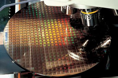
The semiconductor manufacturer is reportedly conducting risk trial production at its Baoshan facility in Hsinchu, northern Taiwan, where it has implemented a new nanosheet architecture that promises a significant advancement over the current 3nm FinFET process. The company plans to transfer this production experience to its Kaohsiung plant for mass manufacturing, according to the report.

TSMC's progress bodes well for Apple, with a September report from analyst Ming-Chi Kuo and a more recent rumor claiming that Apple's 2026 iPhone 18 Pro models will exclusively feature chips built on TSMC's 2nm process and 12GB of RAM. The standard iPhone 18 models are expected to continue using an enhanced 3nm process due to cost considerations.

The 2nm process is said to be generating substantial interest from potential customers, particularly in the AI sector. Indeed, company CEO C.C. Wei has noted unexpectedly high demand for the upcoming 2nm technology, suggesting production at scale will be ramped up as soon as is possible to meet that demand.

TSMC's roadmap includes the 2026 introduction of an A16 process (1.6nm-class – not to be confused with Apple's chip nomenclature), which will combine Super Power Rail (SPR) architecture with nanosheet transistors. SPR is expected to provide an 8% to 10% performance increase at the same voltage and complexity, a 15% to 20% power demand decrease at the same frequency and transistor count, and a 7% to 10% chip density increase, depending on the design.

Tag: TSMC

Popular Stories

m5 macbook pro deal

Why You Shouldn't Buy the Next MacBook Pro

Tuesday February 10, 2026 4:27 pm PST by
Apple is planning to launch new MacBook Pro models as soon as early March, but if you can, this is one generation you should skip because there's something much better in the works. We're waiting on 14-inch and 16-inch MacBook Pro models with M5 Pro and M5 Max chips, with few changes other than the processor upgrade. There won't be any tweaks to the design or the display, but later this...
iOS 26

Apple Releases iOS 26.3 and iPadOS 26.3

Wednesday February 11, 2026 10:07 am PST by
Apple today released iOS 26.3 and iPadOS 26.3, the latest updates to the iOS 26 and iPadOS 26 operating systems that came out in September. The new software comes almost two months after Apple released iOS 26.2 and iPadOS 26.2. The new software can be downloaded on eligible iPhones and iPads over-the-air by going to Settings > General > Software Update. According to Apple's release notes, ...
Apple Logo Zoomed

Apple Expected to Launch These 10+ Products Over the Coming Months

Tuesday February 10, 2026 6:33 am PST by
It has been a slow start to 2026 for Apple product launches, with only a new AirTag and a special Apple Watch band released so far. We are still waiting for MacBook Pro models with M5 Pro and M5 Max chips, the iPhone 17e, a lower-cost MacBook with an iPhone chip, long-rumored updates to the Apple TV and HomePod mini, and much more. Apple is expected to release/update the following products...
iPhone 16e Bottom Crop

Apple Reportedly Unveiling a New iPhone Next Week

Tuesday February 10, 2026 1:51 pm PST by
Apple plans to announce the iPhone 17e on Thursday, February 19, according to Macwelt, the German equivalent of Macworld. The report said the iPhone 17e will be announced in a press release on the Apple Newsroom website, so do not expect an event for this device specifically. The iPhone 17e will be a spec-bumped successor to the iPhone 16e. Rumors claim the device will have four key...
Apple Logo Black

Apple Acquires New Database App

Wednesday February 11, 2026 6:44 am PST by
Apple acquired Canadian graph database company Kuzu last year, it has emerged. The acquisition, spotted by AppleInsider, was completed in October 2025 for an undisclosed sum. The company's website was subsequently taken down and its Github repository was archived, as is commonplace for Apple acquisitions. Kuzu was "an embedded graph database built for query speed, scalability, and easy of ...

Top Rated Comments

16 months ago
Cancelled my iPhone 17 preorder.
Score: 13 Votes (Like | Disagree)
16 months ago

meanwhile intel is rumored to be at 10% yield on 18A
There are two major inputs to yield. Defect density and size of the die. Larger dies have lower yield rates for the same defect density.

Intel has reported that they have about 0.4 defect density ( before HVM status. )

" ... Generally, it is considered that a defect density below 0.5 defects per square centimeter is a good result, so even keeping in mind that defect density varies by process and application, Intel 18A’s defect density of 0.4 defects per square centimeter is a reasonably good result considering its timing. Yet, TSMC’s N7 and N5 technologies had a defect density of 0.33 at a similar development stage, and when TSMC’s N5 reached mass production, its defect density dropped to 0.1. Yet, TSMC’s N3 started with a higher defect density but matched N5’s defect rate after five to six quarters ..."
https://www.tomshardware.com/tech-industry/broadcom-disappointed-with-intel-18a-process-technology-says-its-not-currently-viable-for-high-volume-production


https://semianalysis.com/die-yield-calculator/

For the nominal die settings for the above calculator, 0.4 gives a yield rate of 77% . No where near 10%.

However if try to make reticle busting sized dies that are popular with Nvidia and Broadcom that has problems. For example 25 mm x 30 mm dies drop all the way to ... wait for it .... 10% . Coincidence or source of the disconnect?

[ NOTE: if move that 25 mm x 30 mm die to 0.3 defect rate it jump to 15%. ]


The implementation design is also another factor. ( e.g., Nvidia had to tweak Blackwell to get around some packing yield issues. ) Don't need 'perfect' dies to have a binned working product if have some redundancies . It is more straightforward cheaper to have a lower defect density.


Is TSMC talking reticle sized test dies for their 60% ? Nope. Pretty decent chance what we have here is 'apples to oranges' stuff. Semiaccurate and Korean ( possible Samsung Foundry fans ) throwing 'doom and gloom' at Intel. Intel is off from TSMC's defect density, but 10% is suggestive that probably not talking standard test dies.

18A would not be a good match for Apple because Apple isn't big on chiplets. The 'Max' variant is a relatively big die ( not in the reticle busting zone, but 'big'. ). The huge potential problem for Intel is that their data center dies have tended to run somewhat large ( AMD is making more true chiplets to compose their solutions). 0.4 would make it hard to be profitable unless they start using substantively smaller dies as basic building blocks.

It also cuts Intel out as being a "mega AI die" boundary options. The boundary isn't going to be able to ride the AI hype train. Broadcom probably is twitchy if not doing chiplets ( glue two 600+ mm^2 dies together isn't really 'good' chiplet design. It is really just a means of making something 'even bigger' rather than functional decomposition. ). It is going to be hard for Intel to quickly get some "cost doesn't matter" AI clients in the intermediate term. Nor will their discrete GPU comes back in quicker ( if it survives).

The short term problem for the Intel foundary is that the still only have 'one' big customer. The client PC SoC shop that wants keep the single threaded drag racing crown and the expensive multicore crown. 18A might work well enough for that. But it isn't what the upper 20% die sized folks are looking for. It is a better fit for perhaps folks ding RISC-V / Arm speciality SoCs that are not trying to bust into the datacenter AI/HPC market.

Intel has lots more work to do on better design kits and ecosystem, for broad ranging fab offerings , and establishing expectations with external customers. But 10% yield is likely is just 'doom and gloom' that sells clicks and ad (click bait).
Score: 6 Votes (Like | Disagree)
bodonnell202 Avatar
16 months ago

A very long time ago, I remember hearing a report on public radio saying that the semiconductor industry had an insurmountable barrier to overcome: due to the laws of physics and the wavelength limitations of light energy when etching the silicon wafer through a stencil, there was a 13nm chip size limit. Something tells my memory is faulty, or I missed the technological changes which have happened.
Yes, however a couple decades ago many of the chip manufacturers (not Intel initially, but they are doing it now too to sound competitive) starting using marketing terms to name their manufacturing processes and while chip density has continued to increase the density isn't as much as the name would suggest. For example the N3E which Apple currently uses in the A18 and M4 chips has a transistor gate pitch of 48 nm and an an interconnect pitch of 23 nm so they haven't actually reached the physical limits of what you can do with silicon yet.
Score: 4 Votes (Like | Disagree)
BelgianChoklit Avatar
16 months ago

Cancelled my iPhone 17 preorder.
These have gone old...
Score: 3 Votes (Like | Disagree)
16 months ago
meanwhile intel is rumored to be at 10% yield on 18A
Score: 3 Votes (Like | Disagree)
16 months ago
My wife were planning on trying to keep our phones until at least the 18 series so this sounds good to me.
Score: 2 Votes (Like | Disagree)